Low-power wireless communication with ambient backscattering
Wireless communication without a dedicated transmitter
Ambient backscattering is an especially low-power form of wireless communication for IoT systems. Instead of generating its own RF signal, a backscatter modulator uses ambient radio sources such as Wi‑Fi or Bluetooth and conveys data by deliberately changing the antenna impedance. This article covers the physical operating principle, the practical lab setup, PCB design, signal processing with SDR and a matched filter, and real measurements of bit error rate, range, and minimum impedance change.
What this article covers
- how ambient backscattering works without a dedicated transmitter
- how a backscatter modulator with antenna is built in practice
- the role of RF switches, SDR, and matched filtering
- how bit error rate, range, and power consumption behave
Introduction
Many modern IoT devices must run for long periods with minimal energy use. For battery-powered sensors in particular, replacing batteries is often difficult or impossible.
A large share of power goes to transmitting radio signals, because conventional radio modules must generate their own RF carrier.
An alternative is ambient backscattering: the device does not transmit its own signal but uses ambient radio waves—for example Wi‑Fi or Bluetooth.
Data is sent by changing the antenna impedance, which modulates the reflected signal.
Key advantage:
Energy is not spent generating a carrier—only on switching the antenna.
That enables ultra-low-power communication systems—ideal for IoT with very long runtime.
Operating principle of ambient backscattering
Ambient backscattering does not create its own RF carrier. The system uses existing ambient waves and deliberately changes how they are reflected.
In simplified terms:
- An external source—for example a Wi‑Fi router—transmits an RF signal.
- The backscatter device changes its antenna impedance.
- That changes how strongly the incident wave is reflected.
- A receiver measures the change and reconstructs the transmitted data.
The two impedance states typically map to bit values 0 and 1. Information is conveyed not by an active transmitter but by switching the antenna.
Physically, interference arises between the direct signal from the external source and the signal reflected by the backscatter tag. Depending on the antenna impedance state, the received signal is enhanced or weakened.
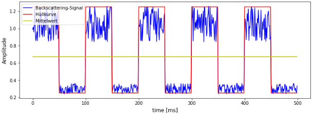
The amplitude—or envelope—of the received signal changes slightly. A receiver can use that change to distinguish the two states and thus bit 0 and bit 1.
A simple approach uses a threshold: if the measured envelope is above a defined mean, it can be interpreted as bit 1; if below, bit 0 is detected.
Ambient backscattering thus enables very low-power wireless links, because only the antenna impedance must be switched—no dedicated RF transmitter is required.
System design and technical choices
The backscatter system was split into sub-problems and each was given a suitable solution, yielding a practical and efficient architecture.
Key design parameters:
- Antenna type
- Modulator circuit
- Modulation scheme
- Receive chain
- Frequency band
Antenna
The lab prototype used a simple λ/4 monopole—easy to build and good for first experiments. A larger antenna structure would help increase reflected power in an optimized design.
Receiver
A software-defined radio (SDR) was used so filtering, demodulation, and processing can be adapted in software without changing hardware.
Modulator
In the lab, a MOSFET switched antenna impedance—it is low power and switches quickly.
At higher frequencies, especially in the Wi‑Fi band, RF switches are preferable: they are designed for RF and show fewer parasitic effects.
Modulation
The first step used amplitude shift keying (ASK)—simple to implement and well suited to experiments.
For more robust links, frequency shift keying (FSK) can reduce sensitivity to amplitude noise and lower BER.
Frequency choice
Experiments used the 2.4 GHz band, widely available from Wi‑Fi and Bluetooth.
The backscatter switching rate is far below the carrier—typically kHz to MHz—so changes are reliably detected.
Lab setup for 1-bit transmission
A simple lab demonstrator was built to transmit a single bit via ambient backscattering.
The setup consists of:
- Microcontroller (TinyK22)
- MOSFET (2N7000)
- λ/4 monopole (wire)
The MCU drives the MOSFET, which periodically ties the antenna to ground, changing impedance and modulating the reflected RF.
Drive side
The MCU toggles a GPIO pin between logic 0 and 1, turning the MOSFET on and off.
Switching rate is set with a simple delay loop; varying it shows under which conditions the backscatter signal is easiest to detect.
Antenna
A λ/4 monopole is used—about 3 cm long at 2.4 GHz.
With the ground plane it behaves like a virtual dipole; impedance switching deliberately changes reflection.
Reception with SDR and simple processing (lab)
The signal is captured with an SDR and processed in software.
Processing steps:
- Magnitude / envelope detection
- Mean computation
- Compare envelope to the mean
- Detect state changes (bit transitions)
Because reflection can cause constructive or destructive interference depending on position, bit polarity cannot be determined directly.
A preamble therefore calibrates mapping from signal state to bit value (0 or 1).
Why software-defined radio?
An SDR replaces classic analog front ends with digital processing—filtering, demodulation, and detection run in software.
The system stays flexible and can be retuned for different frequencies, modulations, and experiments.
Physical model and hypotheses
Physical relations are stated mathematically; four central hypotheses guide the experimental setup.
Hypothesis 1: signal change via interference
The received signal is the superposition of a direct path and a reflected path:
s(t) = a₁ · ejω(t−τ₁) + a₂ · ejω(t−τ₂)
Here a₁ and a₂ are the path gains and τ₁, τ₂ the delays.
Phase shift follows from path length ℓ:
φ = 2π · ℓ / λ
Depending on phase difference, interference is constructive or destructive:
- Constructive: φ ≈ 0 → signal boost
- Destructive: φ ≈ π → signal reduction
Switching antenna impedance changes a₂, which modulates the overall amplitude.
Hypothesis 2: position dependence
Delays τ₁ and τ₂ follow path lengths ℓ₁ and ℓ₂:
τ = ℓ / c
Hence the phase shift:
φ = 2π · (ℓ₂ − ℓ₁) / λ
A position change of only:
Δℓ = λ / 2
yields a π phase shift and toggles between constructive and destructive interference.
Mapping signal change to bit value (0 or 1) is therefore position-dependent and must be learned via a preamble.
Hypothesis 3: antenna and reflection
Reflected power scales with power at the antenna:
P ∝ A · E²
where A is effective aperture and E electric field strength.
The reflection coefficient Γ sets reflection strength:
Γ = (ZL − Z0) / (ZL + Z0)
A larger impedance change ΔZ yields a larger |Γ| and stronger modulation of the reflected wave.
Hypothesis 4: envelope detection
For detection the received signal is converted to its envelope:
senv(t) = |s(t)|
Then a mean is formed:
μ = (1/N) · Σ senv(t)
Bit decisions use a threshold comparison:
senv(t) > μ → Bit = 1
senv(t) < μ → Bit = 0
A state change is seen when the envelope crosses the mean periodically. Detection depends on switching frequency and sample rate.
These four hypotheses underpin experimental validation of the backscatter system.
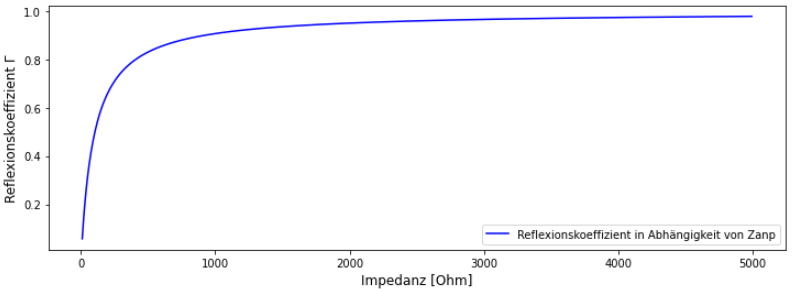
Minimum impedance change
A central question is how large the impedance change must be so the resulting reflection remains detectable at the receiver.
Split between absorbed and reflected energy is described by the reflection coefficient:
Γ = (Zant − Z0) / (Zant + Z0)
Z0 is system impedance (typically 50 Ω) and Zant antenna impedance.
Special cases:
- Zant = Z0 → Γ = 0 → matched (no reflection)
- Zant → 0 Ω → Γ → −1 → full reflection
- Zant → ∞ → Γ → +1 → full reflection
Maximum backscatter modulation needs two states:
- low reflection (matched)
- high reflection
Effect of impedance change
In practice antenna impedance is altered via a matching network:
Zant = Z0 + Zanp
Modulation strength depends directly on how Zanp changes.
The magnitude of the reflection coefficient is:
|Γ| = |(Zant − Z0) / (Zant + Z0)|
|Γ| grows with impedance swing but with diminishing returns.
Practical result
Measurements show that at roughly 1000 Ω a reflection coefficient of:
|Γ| ≈ 0.9
is already reached.
Further increasing impedance yields little extra gain as |Γ| asymptotically approaches 1.
Conclusion
The minimum impedance swing depends on how much reflection contrast is needed for reliable detection.
Moderate changes already capture most of the available reflection, so the modulator can be built efficiently and with modest effort.
The following experiments verify these findings on the assembled system.
Test setup and experimental results
A 1-bit demonstrator was built and refined step by step to test the hypotheses.
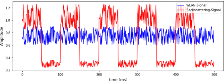
Issue: unstable Wi‑Fi signal
The first trial used Wi‑Fi as the external source. The signal fluctuates strongly and does not transmit continuously.
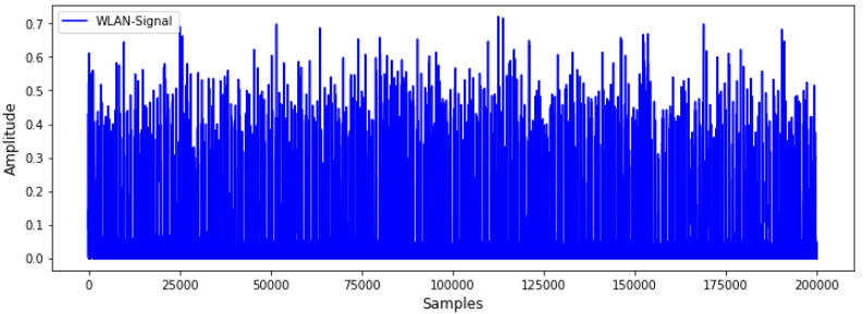
WLAN amplitude swings then mask the backscatter effect, so switching points are hard to detect reliably.
Reference run with constant carrier
To avoid that, a constant carrier was generated with a software-defined radio.
The backscatter effect then becomes clearly visible.
- Switching produces measurable amplitude changes
- Changes are clearly distinct from the baseline
Hardware impact
Two options were tested for switching antenna impedance:
- Push button: clear, repeatable signal changes
- MOSFET: smaller amplitude swing and less stable switching
The MOSFET behaves capacitively at high frequency, so signal partly leaks through even when “off.”
Antenna and position
Geometry has a strong effect:
- Larger antennas give stronger reflections
- A ground plane noticeably boosts signal level
- Antenna position strongly affects interference
Depending on position, interference is constructive or destructive and the amplitude changes.
Results
Under controlled lab conditions:
- Backscatter produces measurable modulation
- Hypotheses on interference and antenna behavior hold
- Detection depends heavily on signal stability and hardware
Conclusion
Using WLAN as carrier is limited because of strong fluctuations.
Reliable detection needs:
- as constant a carrier as possible
- stable antenna impedance switching
- optimized processing (e.g. matched filter)
The next build therefore uses an RF switch instead of a MOSFET for clean, repeatable toggling.
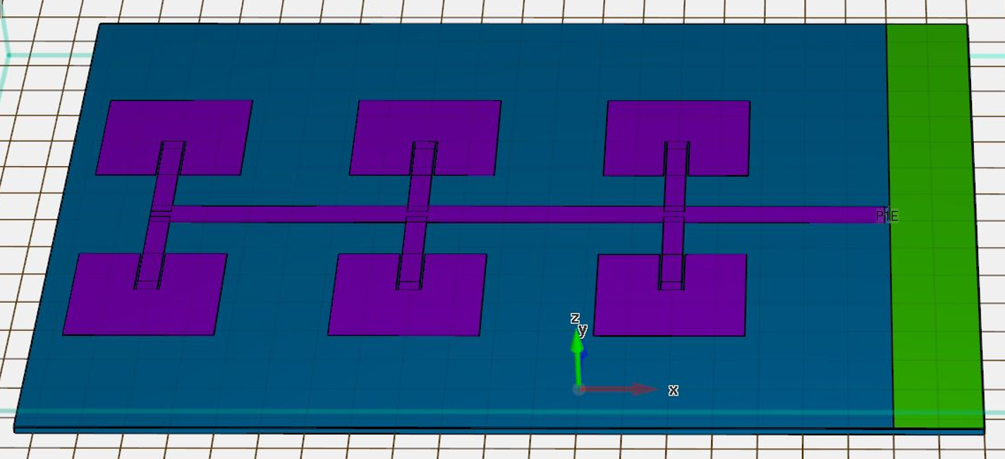
From lab to antenna: patch design and RF simulation
Based on lab lessons the modulator was refined and implemented as a PCB.
The goal was to maximize reflection while keeping modulation stable and repeatable.
Antenna
Where the lab used a simple monopole, the final design uses a patch array.
It offers larger effective area and stronger backscatter.
The antenna is tuned near 2.4 GHz to use the Wi‑Fi band efficiently.
Matching and reflection
Efficient operation needs good antenna matching—target impedance near the system value:
Z ≈ 50 Ω
Simulated antenna impedance:
Z = 46.1 + j2.02 Ω
That is a good match and minimizes loss.
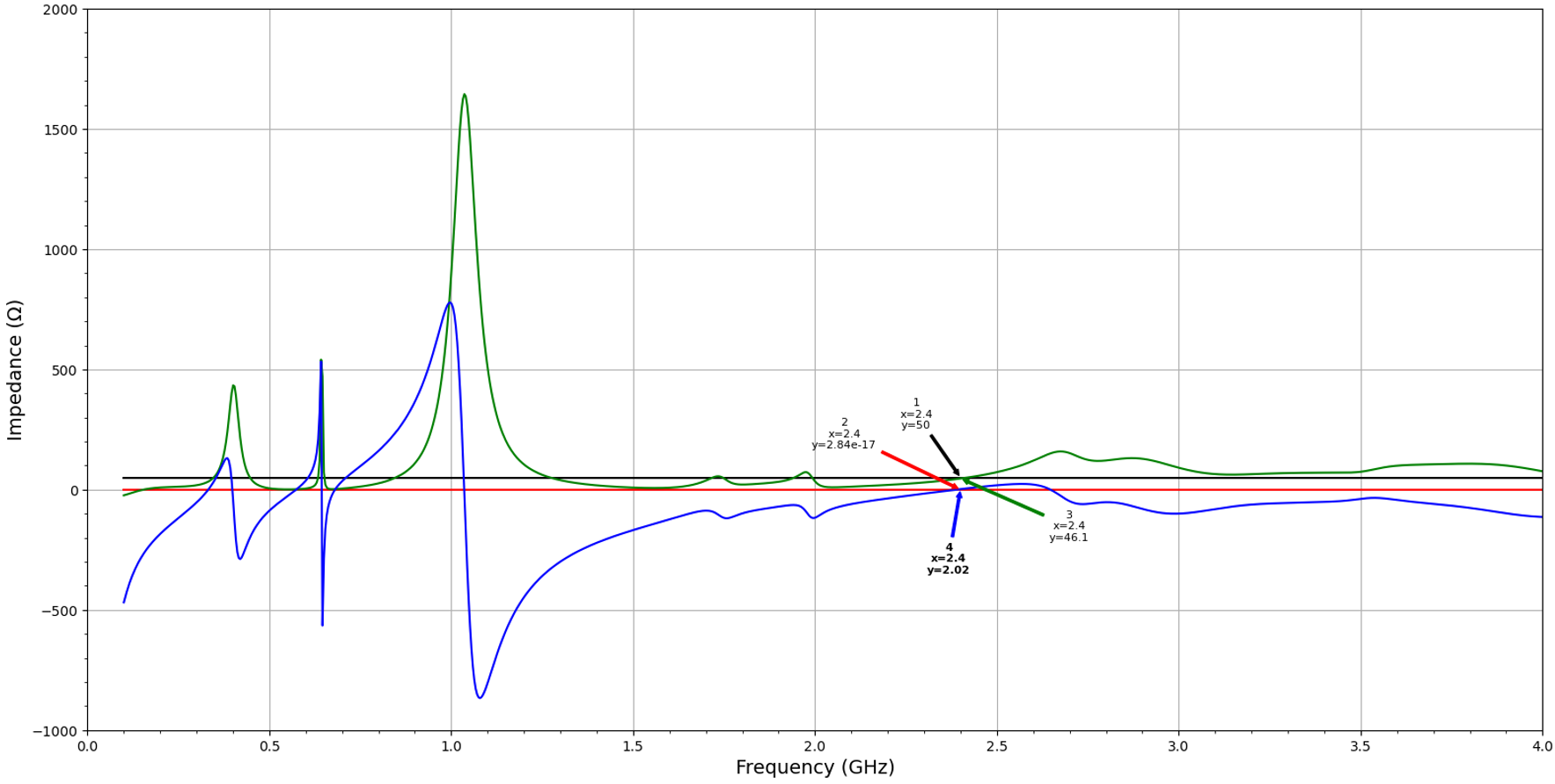
Match quality is described by reflection factor / S-parameter:
S11 = 20 · log10(|Γ|)
For this antenna:
- at 2.4 GHz: S11 < −26 dB
- at 2.5 GHz: S11 ≈ −12.6 dB
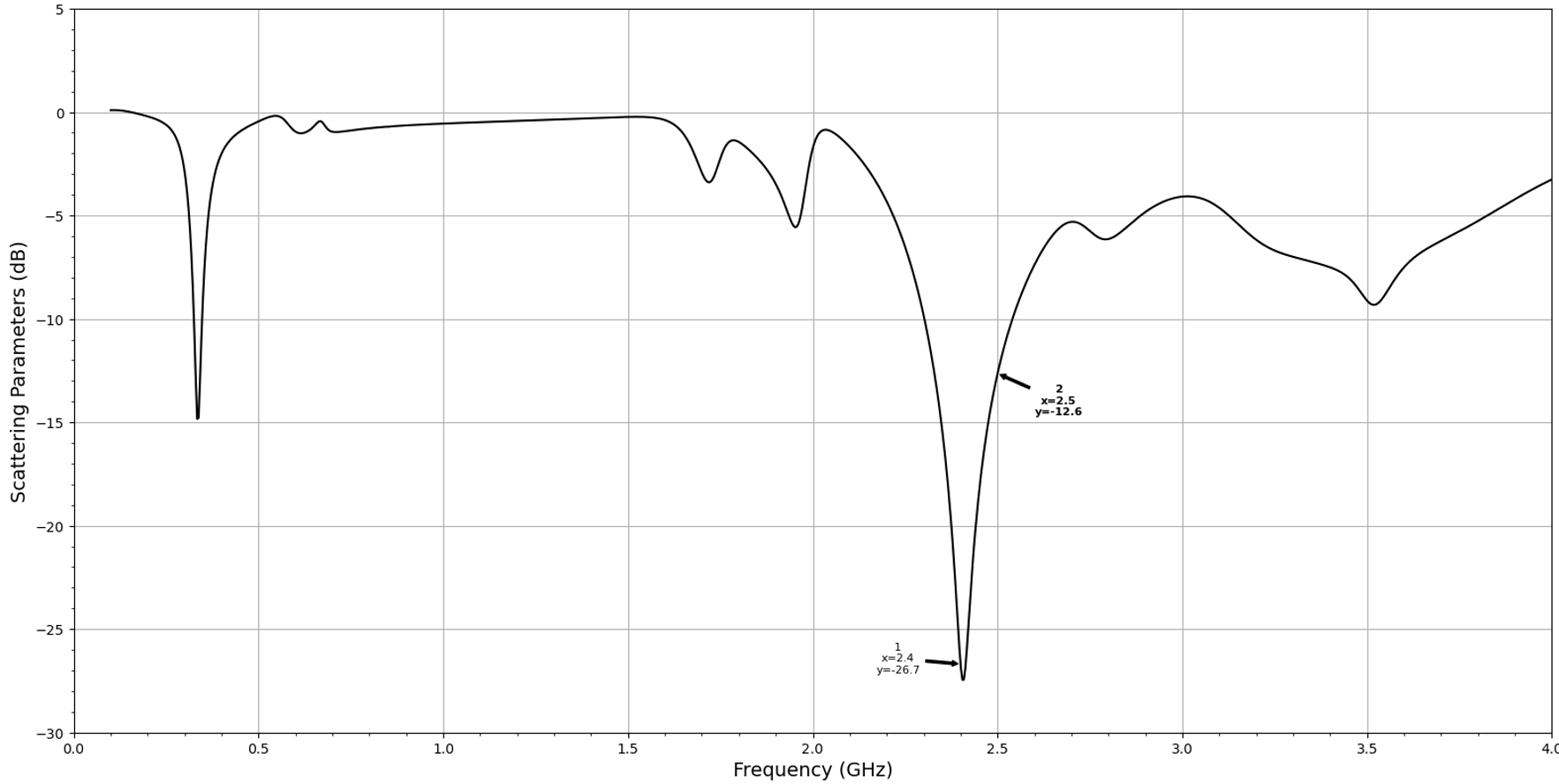
The full Wi‑Fi band is covered adequately.
Implications for backscatter
Low S11 means good match and little reflection in the default state.
Deliberate impedance changes in the modulator can swing Γ strongly:
Γ = (ZL − Z0) / (ZL + Z0)
That yields a clear difference between the two switch states for data transfer.
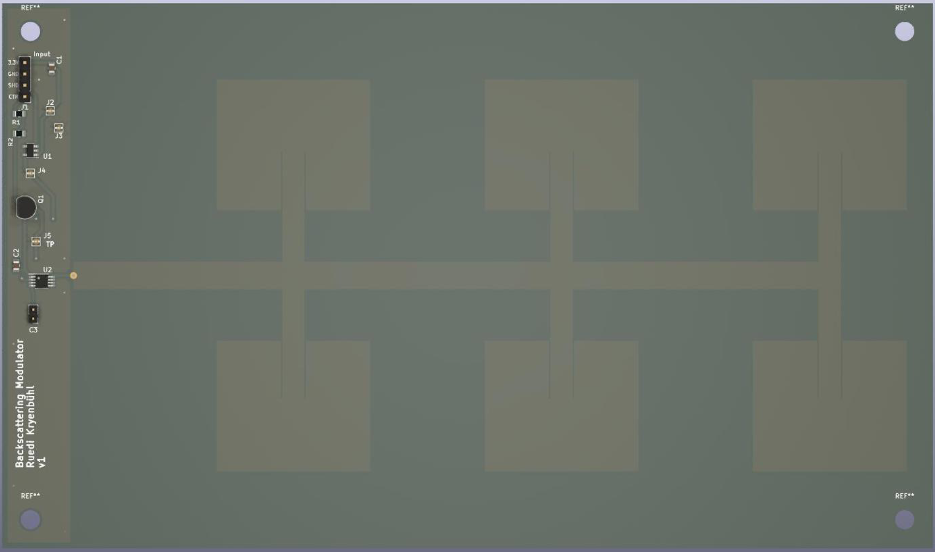
PCB integration
The antenna is etched as copper geometry on the board—a compact system without a separate antenna.
Geometry is reproducible and electrical behavior is more stable than a wire prototype.
Modulator hardware: RF switch, supply, and PCB
The modulator was further developed as an integrated PCB.
Modulator design
The lab MOSFET was replaced by an RF switch (ADG902).
The switch is intended for RF and offers:
- lower parasitics
- clean isolation when off
- more consistent impedance switching
That yields a larger, more stable contrast in antenna reflection.
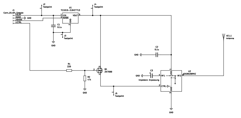
Voltage conditioning
The MCU runs at 3.3 V while the RF switch expects lower drive; a converter is used:
- Output: about 2.75 V
- Type: TC1015
It has a shutdown input to cut idle power.
For energy-optimized IoT, such conversion should ideally be avoided—it adds loss.
Variable matching
An external pad was added to vary matching and study minimum impedance change vs. detectability.
The impedance–signal relation can be explored directly in hardware.
PCB layout
The full system is on one board.
- Left: modulator circuit
- Right: integrated patch antenna
Integrating the antenna on the PCB gives:
- defined geometry
- repeatable electrical behavior
- compact form factor
Improvements over the lab build
RF switch plus integrated antenna address the main weaknesses of the breadboard setup:
- more stable impedance switching
- larger amplitude contrast
- better repeatability
The PCB is the basis for reliable ambient backscatter data transfer.
Receiver algorithm: preamble, matched filter, and bit decision
Backscatter data is detected by digitally processing the received signal step by step.
Frame detection and preamble
To find packet start, a known preamble bit pattern prefixes the data:
P = [0, 1, 1, 1, 0, 1, 0, 1]
The received signal is correlated with this preamble:
R(τ) = Σ s(t) · p(t − τ)
A correlation peak marks the preamble position and synchronizes to the data frame.

Signal conditioning
The received signal can fluctuate strongly, especially with Wi‑Fi as carrier.
Several filters were evaluated:
- Moving average
- Low-pass
- Matched filter
The matched filter works best because it aligns to the expected pulse shape:
y(t) = s(t) * h(t)
where h(t) is the time-reversed conjugate reference pulse.
That improves SNR and amplifies amplitude differences between bits.
Bit detection
Data uses amplitude shift keying (ASK).
The signal envelope is computed:
senv(t) = |s(t)|
Instead of comparing single samples, averages are taken over each bit interval:
μbit = (1/N) · Σ senv(t)
Decisions compare to the global mean:
μbit > μ → Bit = 1
μbit < μ → Bit = 0
Averaging reduces sensitivity to short-term amplitude swings and improves BER.
Synchronization
Correct detection needs accurate timing alignment.
Small frequency offset between source and receiver can drift the sampling instant.
An early–late gate synchronizer corrects that.
Two samples are compared:
- early sample
- late sample
Their difference forms an error signal:
e = s(t + Δ) − s(t − Δ)
If e ≠ 0, the sampling time is adjusted.
After matched filtering the waveform is roughly triangular, so timing error is easy to see.
Summary
Together:
- Matched filter
- Preamble correlation
- Mean-based bit decision
- Early–late synchronization
enable robust detection despite small amplitude swings and strong noise.
Measurement results: waveforms, frame transfer, and WLAN carrier
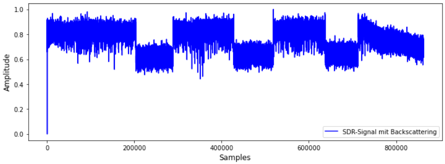
Several measurement runs verified the modulator and exercised the full processing chain. Tests used about one meter separation between receiver and RF source.
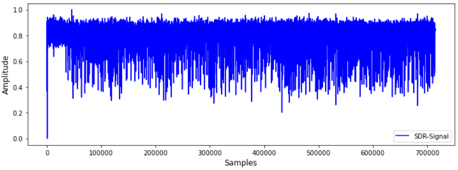
Detection with constant carrier
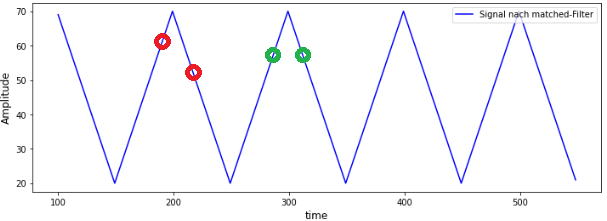
The first run used a constant RF carrier. With 100 ms switching time, changes are clearly visible.
A matched filter further boosts amplitude contrast:
y(t) = s(t) * h(t)
At 10 ms switching, raw traces no longer show visible changes.
After matched filtering, transitions reappear—highlighting the need for DSP.
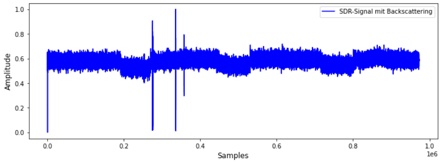
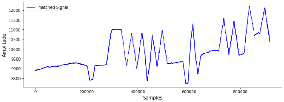
Preamble detection and data transfer
The received signal is correlated with the known preamble:
R(τ) = Σ s(t) · p(t − τ)
A peak marks the frame position.
The test word PAIND was transmitted; the receiver produced:
PAIND → PAAFD
yielding 2 bit errors.
A frame consists of the known 8-bit preamble plus payload. PAIND was encoded as 40 payload bits (5 ASCII characters); the stated BER refers to those payload bits in the evaluated frame. The preamble is for sync only and is excluded from that error rate.
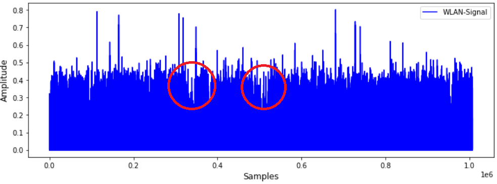
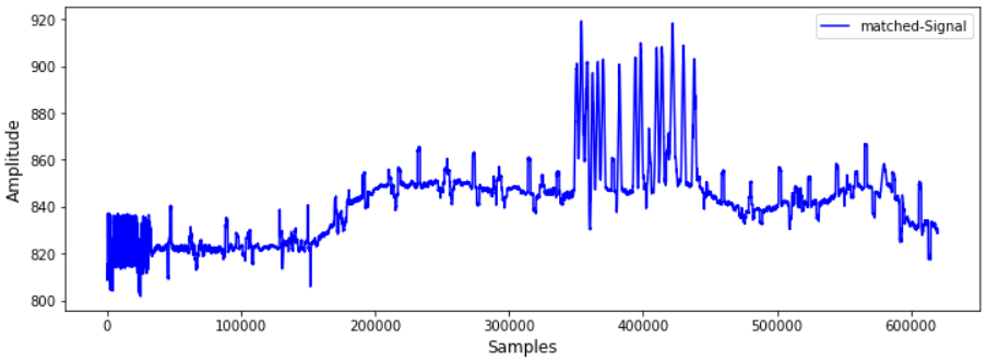
Transfer with WLAN carrier
With a real Wi‑Fi carrier:
- At 10 ms switching, detection was unreliable
- At 100 ms, detectable but higher error rate
Measured BER:
BER = 9 / 40 = 0.225
Again the denominator is the same 40 payload bits (preamble excluded).
Higher errors follow strong WLAN amplitude variation.
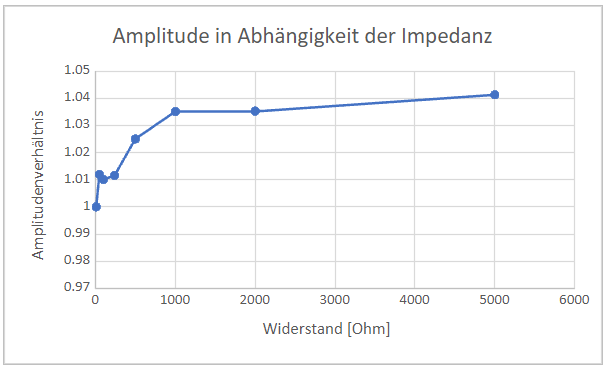
Minimum impedance swing measurement
Various resistors were tried to map impedance change vs. amplitude ratio.
Results match the model:
- Near 1000 Ω, about 90% of maximum amplitude is reached
- Below roughly 50 Ω, no clear change is detectable
Impedance impact follows the reflection coefficient:
Γ = (ZL − Z0) / (ZL + Z0)
Summary
Measurements show:
- Backscatter works reliably under lab conditions
- Processing (matched filter) is critical
- WLAN as carrier works but is error-prone
- Impedance swing directly sets detectability
The modulator’s behavior is thus confirmed experimentally.
System figures and overall assessment
Key metrics analyzed: power draw, BER, range, and bitrate.
Power consumption
Ambient backscatter’s main advantage is extremely low power—no dedicated RF transmitter.
Component power estimates:
- RF switch: 1 µA · 2.75 V → 0.003 mW
- Voltage converter: 0.08 mA · 3.3 V → 0.26 mW
- MOSFET (reference): 0.283 mW
Total power:
P = U · I
approximately:
Ptotal ≈ 0.546 mW
Much of the loss is voltage conversion. With an ideal design without a converter, power can drop to a few microwatts:
P ≈ 3 µW
That suits energy-harvesting IoT well.
Bit error rate (BER)
BER is the ratio of erroneous bits to total bits:
BER = Nerror / Ntotal
In one campaign:
- 600 bits transmitted
- 42 errors detected
Hence:
BER = 42 / 600 ≈ 0.07
Error correction can reduce BER—for example with a Hamming code:
BER ≈ 0.036
More redundancy can reduce it further.
Range
Maximum detectable range was about:
d ≈ 2 m
Tests and data transfer used ~1 m; BER increased with distance.
Compared with Bluetooth Low Energy (10–40 m typical), range is much shorter.
Limits come from:
- low reflected power
- strong geometry dependence
- multipath
Bitrate
Achieved data rate:
R ≈ 100 bit/s
Enough for simple sensor telemetry, e.g. periodic readings.
Higher throughput needs better modulation and processing.
Overall assessment
Ambient backscatter is a working, extremely energy-efficient link technology.
- Sub-µW power is feasible
- Data transfer was demonstrated
- Range and rate are limited
Best suited when efficiency matters more than high rate or long range.
Meeting the target (bits transmitted)
The goal was to show that ambient backscatter can reliably deliver at least 8 bits.
Constant-carrier results
With a constant external carrier (SDR), 40 payload bits were sent (frame test as above).
Only 2 bit errors occurred:
BER = 2 / 40 = 0.05
The 8-bit requirement is clearly exceeded; simple FEC can reduce errors further.
WLAN-carrier results
With real Wi‑Fi carrier, 40 payload bits were evaluated.
9 bit errors were observed:
BER = 9 / 40 = 0.225
Higher errors follow non-constant amplitude and Wi‑Fi burst structure.
Assessment
Results show:
- Ambient backscatter fundamentally works
- The 8-bit target is far exceeded
- Controlled carrier transfer is reliable
- Wi‑Fi carrier needs more optimization
Practical IoT use still needs robustness to real, fluctuating carriers.
Conclusion and outlook
This work shows ambient backscatter can carry data in principle.
With the developed modulator, data was sent over an external carrier. Four hypotheses were confirmed:
- Impedance-based modulation works
- Interference yields measurable amplitude changes
- Antenna pattern strongly affects signal strength
- Detected changes can carry bits
Ambient backscatter is validated as an energy-efficient communication method.
Optimization potential
Further work for real IoT deployment:
- Antenna design: shrink size without badly hurting reflection.
- Signal robustness: stabilize links over real carriers like Wi‑Fi with strong fading.
- Modulation: FSK can improve robustness to amplitude variation.
- Error correction: block codes, CRC, or ARQ help clean up residual errors.
System behavior and challenges
Experiments show strong dependence on geometry.
Multipath and interference make quality position-sensitive; small antenna moves toggle constructive/destructive combining.
Practical systems may need algorithms that find good placement automatically or adapt to conditions.
Outlook
Ambient backscatter has strong potential for future energy-autonomous IoT, especially for very low power and low rate.
Better antennas, robust DSP, and coding can push the approach toward real deployments.
Author: Ruedi von Kryentech
Created: 6 Apr 2026 · Last updated: 6 Apr 2026
Technical content as of the last update.